New process creates 15-times-faster memory in 90 percent smaller package.
IBM and Micron Technology, Inc. announced today that Micron will begin production of a new memory device built using the first commercial CMOS manufacturing technology to employ through-silicon vias (TSVs). IBM's advanced TSV chip-making process enables Micron's Hybrid Memory Cube (HMC) to achieve speeds 15 times faster than today's technology.
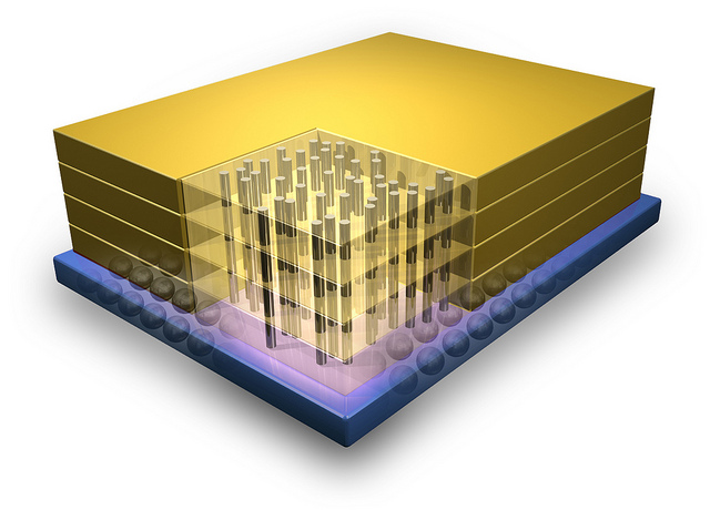
Micron's Hybrid Memory Cube features a stack of individual chips connected by vertical pipelines or “vias,” shown above. IBM’s new 3-D manufacturing technology, used to connect the 3D micro structure, will be the foundation for commercial production of the new memory cube.
IBM will present the details of its TSV manufacturing breakthrough at the IEEE International Electron Devices Meeting December 5 in Washington, DC.
HMC parts will be manufactured at IBM's advanced semiconductor fab in East Fishkill, N.Y., using the company's 32nm, high-K metal gate process technology.
 Micron's Hybrid Memory Cube features a stack of individual chips connected by vertical pipelines or “vias,” shown above.
HMC will enable a new generation of performance in applications ranging from large-scale networking and high-performance computing, to industrial automation and, eventually, consumer products.
"This is a milestone in the industry move to 3D semiconductor manufacturing," said Subu Iyer, IBM Fellow. "The manufacturing process we are rolling out will have applications beyond memory, enabling other industry segments as well. In the next few years, 3D chip technology will make its way into consumer products, and we can expect to see drastic improvements in battery life and functionality of devices."
"HMC is a game changer, finally giving architects a flexible memory solution that scales bandwidth while addressing power efficiency," said Robert Feurle, vice president of DRAM Marketing for Micron. "Through collaboration with IBM, Micron will provide the industry's most capable memory offering."
Additional information, technical specifications, tools and support for adopting HMC technology can be found at www.micron.com.
Micron Technology, Inc., is one of the world's leading providers of advanced semiconductor solutions. Through its worldwide operations, Micron manufactures and markets a full range of DRAM, NAND and NOR flash memory, as well as other innovative memory technologies, packaging solutions and semiconductor systems for use in leading-edge computing, consumer, networking, embedded and mobile products. Micron's common stock is traded on the NASDAQ under the MU symbol. To learn more about Micron Technology, Inc., visit www.micron.com.
For more information about IBM's advanced semiconductor products and manufacturing processes visit www.ibm.com/chips
IBM and Micron Technology, Inc. announced today that Micron will begin production of a new memory device built using the first commercial CMOS manufacturing technology to employ through-silicon vias (TSVs). IBM's advanced TSV chip-making process enables Micron's Hybrid Memory Cube (HMC) to achieve speeds 15 times faster than today's technology.
Micron's Hybrid Memory Cube features a stack of individual chips connected by vertical pipelines or “vias,” shown above. IBM’s new 3-D manufacturing technology, used to connect the 3D micro structure, will be the foundation for commercial production of the new memory cube.
IBM will present the details of its TSV manufacturing breakthrough at the IEEE International Electron Devices Meeting December 5 in Washington, DC.
HMC parts will be manufactured at IBM's advanced semiconductor fab in East Fishkill, N.Y., using the company's 32nm, high-K metal gate process technology.

HMC will enable a new generation of performance in applications ranging from large-scale networking and high-performance computing, to industrial automation and, eventually, consumer products.
"This is a milestone in the industry move to 3D semiconductor manufacturing," said Subu Iyer, IBM Fellow. "The manufacturing process we are rolling out will have applications beyond memory, enabling other industry segments as well. In the next few years, 3D chip technology will make its way into consumer products, and we can expect to see drastic improvements in battery life and functionality of devices."
"HMC is a game changer, finally giving architects a flexible memory solution that scales bandwidth while addressing power efficiency," said Robert Feurle, vice president of DRAM Marketing for Micron. "Through collaboration with IBM, Micron will provide the industry's most capable memory offering."
Additional information, technical specifications, tools and support for adopting HMC technology can be found at www.micron.com.
Micron Technology, Inc., is one of the world's leading providers of advanced semiconductor solutions. Through its worldwide operations, Micron manufactures and markets a full range of DRAM, NAND and NOR flash memory, as well as other innovative memory technologies, packaging solutions and semiconductor systems for use in leading-edge computing, consumer, networking, embedded and mobile products. Micron's common stock is traded on the NASDAQ under the MU symbol. To learn more about Micron Technology, Inc., visit www.micron.com.
For more information about IBM's advanced semiconductor products and manufacturing processes visit www.ibm.com/chips


LATEST COMMENTS
MC Press Online